Application Background
In high-performance electronics such as laptops, servers, 5G communication devices, and AI accelerators, packaging structures are becoming increasingly complex, with higher component density and faster data processing.
Coplanarity is a critical assembly parameter that directly impacts electrical connectivity, thermal performance, and product lifespan.
Measurement Challenges
In high-density packaging, closely spaced solder joints are prone to occlusion. Traditional 3D line-scan systems often suffer from blind spots due to projection angle limitations;
Repeatability must be within ±2 μm to ensure consistent and reliable results;
In mass production, measurement cycle time must be less than 8 seconds per part.
Solution Highlights
FPGA-Based Imaging Acceleration
Industrial-grade parallel processing with per-frame speed as fast as 0.14 seconds for high-throughput inspection.
Multi-Projection Structured Light Technology
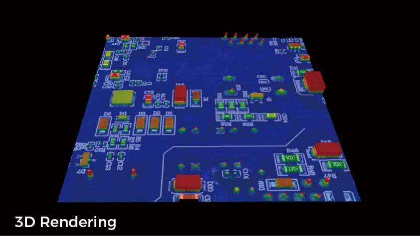
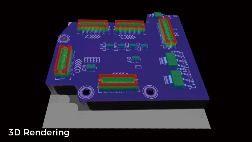
Multi-angle projection eliminates shadows and occlusions, enabling full coverage of pins and solder pads.
Large Field of View with Micron-Level Precision
16.2MP CMOS sensor with 6μm pixel pitch, covering a 53×30.2×20mm³ measurement volume; repeatability < 0.1μm for detecting subtle warping and non-coplanarity.
Telecentric Optics + Combined 2D/3D Measurement
Minimizes angle-related distortion and ensures consistent measurement; pixel-level alignment of 2D textures and 3D point clouds for precise structural reconstruction.
Customer Benefits
Enables blind-spot-free inspection of high-density packages, ensuring reliable solder connections;
Enhances early detection of coplanarity anomalies to prevent cold soldering and thermal failures;
Supports high-speed production lines, improves yield, and optimizes process control.
3D Point Cloud


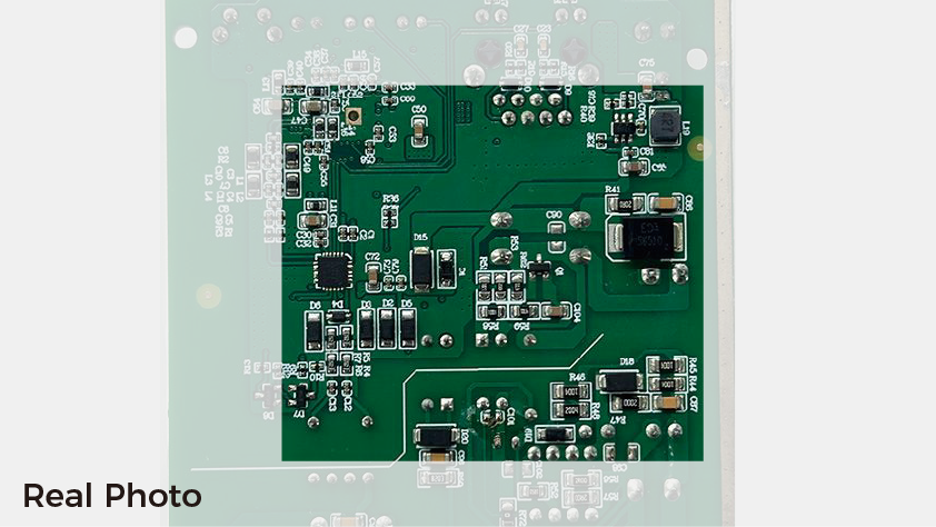
PCBA BOARD


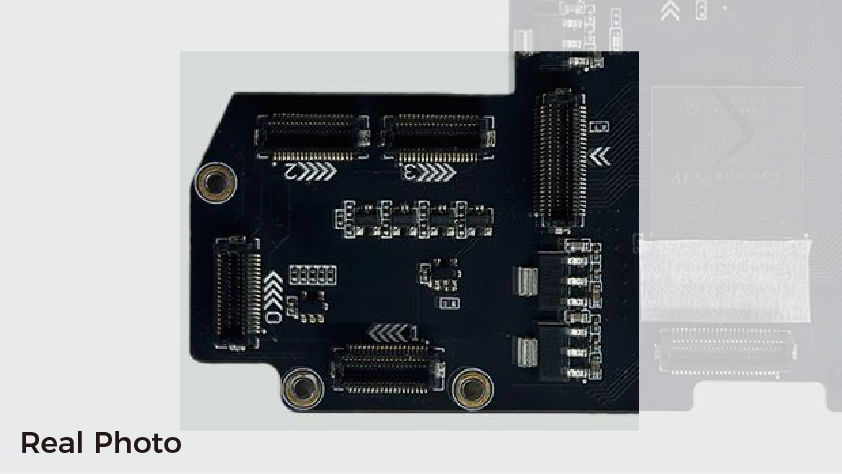
PCBA BOARD
© All images sourced from Mega Phase cameras. Unauthorized replication or misuse is subject to legal claims.

